Your Cart is Empty
In the realm of nanotechnology and materials science, the ability to visualize and analyze structures at the nanoscale is paramount. Scanning Electron Microscopy (SEM) and Transmission Electron Microscopy (TEM) stand as two powerful tools at the forefront of this exploration, each offering unique insights into the microcosmos of materials. In this article, we embark on a comparative journey to understand the differences, strengths, and applications of SEM and TEM.
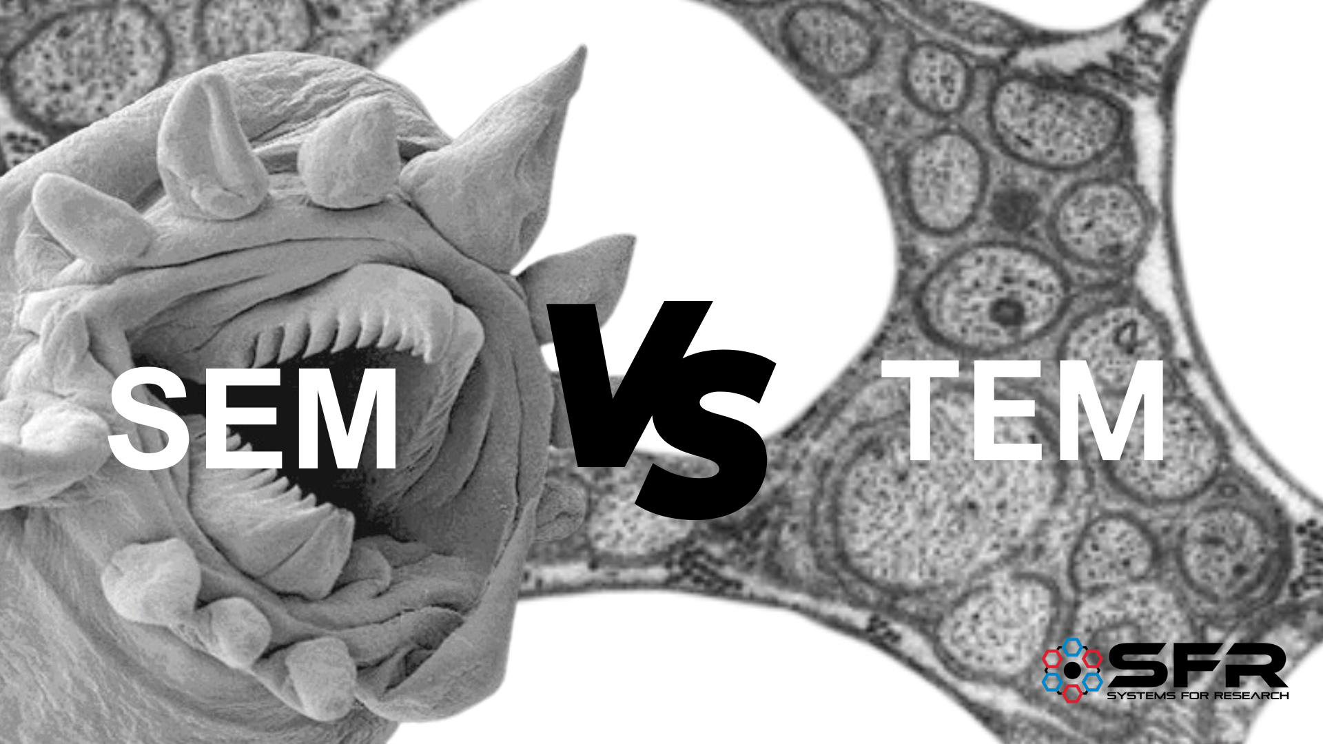
Scanning Electron Microscopy (SEM): Peering into Surface Morphology
At the heart of SEM lies the ability to capture high-resolution images of a material's surface morphology. SEM operates by scanning a focused beam of electrons across the specimen, eliciting various signals such as secondary electrons, backscattered electrons, and X-rays. These signals are then detected and translated into an image, providing intricate details of the surface topography and composition.
The ability of SEM to image a variety of samples, including conductive and non-conductive materials, is one of its main benefits. Moreover, SEM is a recommended option for routine analysis in disciplines like materials science, biology, and geology since it makes sample preparation very simple.
Transmission Electron Microscopy (TEM): Delving into Structural Composition
In contrast to SEM, TEM delves deeper into the structural composition of materials, offering unparalleled insights into atomic-scale features. Instead of scanning the surface, TEM transmits electrons through a thin specimen, creating a highly magnified image of the internal structure. This technique enables researchers to visualize individual atoms, crystal lattices, and defects with extraordinary clarity.
TEM's ability to resolve fine details makes it indispensable in elucidating the microstructure of materials, such as nanoparticles, semiconductors, and biological specimens. However, TEM's sample preparation is more intricate, often requiring ultrathin sections or electron-transparent grids, and its operation demands meticulous control and expertise.
Choosing the Right Tool for the Job
While both TEM and SEM provide priceless insights into the nanoworld, choosing the right method depends on the particular goals of the study as well as the properties of the material. When it comes to surface examination, SEM is excellent at delivering in-depth details about morphology, texture, and elemental composition. Conversely, the strength of TEM is in dissecting the atomic configurations and interior structure of materials.
To get a thorough grasp of a material's properties, researchers frequently use a complimentary strategy, combining TEM and SEM. Surface morphology and structural analysis together open up new creative possibilities for materials science and medicines, among other domains.
Looking Ahead: Advancements in Microscopy
To sum up, SEM and TEM are essential components of contemporary microscopy, providing distinct insights into the complex realm of nanoscale processes. With the use of these instruments, researchers can explore atomic structures and uncover hidden layers of surface morphology, therefore expanding the frontiers of scientific inquiry and creativity.
Come along as we explore the intriguing world of microscopy in more detail, where each pixel reveals a tale just waiting to be told.
