Your Cart is Empty


618-5
"Critical Dimension (CD) structures" are particularly useful for SEM / FIB magnification calibration and may be used for AFM.

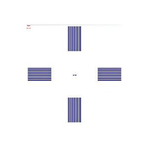
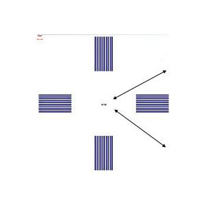
Microscopists and engineers using high performance SEMs or FIB systems will find this calibration test specimen useful. The 4.8 x 4.8mm silicon standard has a series of patterns with a side length of 480µm around its edges, helpful for orientation. There are three versions available.
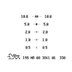
Version with a 10-5-2-1-0.5um structure

This CD calibration test specimen comprises 5 line patterns, each one clearly identified by its pitch. Each pattern has five bars and spaces of equal pitch:10.0um, 5.0µm, 2.0µm, 1.0µm and 0.5µm. The central line area may be used for AFM measurements. The patterns are etched into Si with a depth of approximately 200nm. There is no coating on the Si surface.
Two types are offered:
- non-certified
- certified by PTB (Physikalische Technische Bundesanstalt - German counter part of NIST)
and individually numbered.
Based on the measurement of 9 different standards, the accuracy and uniformity are:
| Pattern Size | 10µm | 5µm | 2µm | 1µm | 0.5µm |
| Accuracy | 0.20% | 0.22% | 0.35% | 0.56% | 0.78% |
| Uniformity | 0.27% | 0.34% | 0.53% | 0.80% | 1.2% |
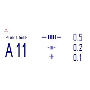
This advanced CD calibration test specimen is suited for calibrating smaller structures. The 500-200-100nm test specimen comprises 3 line patterns, each identified by its pitch. Each pattern has 5 bars and spaces with equal pitch: 500nm, 200nm and 100nm. The central area may be used for AFM measurements. The patterns are etched into Si with a depth of approx. 45-50nm. There is no coating on the Si surface. On some CD calibration targets one of the 100nm lines can be missing. This is a normal occurrence and does not influence performance of the specimen. see mount selections, types A-Q
| Pattern Size | 500nm | 200nm | 100nm |
| Accuracy | 0.30% | 0.55% | 0.50% |
| Uniformity | 0.24% | 0.60% | 1.20% |